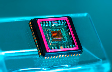

With the increasing scope of functionality of electronic systems and advances in miniaturization, traditional chip designs are coming ever closer to their technological and economic limits. Through novel integration concepts – such as chip stacking or the use of interposers – it is possible to achieve higher data throughput while simultaneously lowering energy consumption and reducing space requirements. Modern packaging solutions up to chiplets also enable the integration of diverse component types, such as processors, sensors and wireless interfaces, in a single module.
Particular challenges in the design process include mastering complexity, optimal utilization of the additional degrees of freedom and consideration of the close thermal, mechanical and electrical coupling in the stacked system. Fraunhofer IIS/EAS can assist you in solving these challenges for an optimized system packaging.
The Chiplet Center of Excellence
Together with Fraunhofer IZM and Fraunhofer ENAS, we have launched a pioneering research initiative: the Chiplet Center of Excellence (CCoE). Together with industry, we drive forward the introduction of chiplet technologies.
Robust chiplet solutions
The innovative chiplet approach offers great potential for the automotive and industrial sectors. The modular principle behind chiplets enables efficient design and production: individual components have to be produced only once and can then be flexibly combined to create tailored solutions.
By integrating various functional units, chiplet technology enhances performance through the opportunity to involve mixed processing nodes from major nodes down to 5nm, as well as more specific technologies such as SiGe and GaN. This offers major advantages when it comes to the cost-effective production of high-performance specialized chips.
Fraunhofer IIS is researching specialized chiplet solutions that meet the requirements for long-term stability and reliability. Particularly with regard to chiplet architectures and design, Fraunhofer IIS supports you in utilizing the advantages of the chiplet approach from concept to prototype realization.
 Fraunhofer Institute for Integrated Circuits IIS, Division Engineering of Adaptive Systems
