Newsletter 02/2017
With investments totaling 350 million euros in their research equipment, the eleven institutes of the Fraunhofer Group for Microelectronics and two institutes of the Leibniz Association participating in the »Research Fab Microelectronics Germany« project will create innovative offerings while more intensively networking their technology know-how and making it available across different sites, all from a single source. With this funding, the Federal Ministry for Education and Research seeks to strengthen the innovative capabilities of the semiconductor and electronics industry in Germany and Europe in the face of global competition and is supporting the project with the largest investment in research equipment since reunification. 100.8 million euros of this forward-looking program are going to the four participating Fraunhofer institutes located in Saxony. Fraunhofer IIS/EAS will bring in its developments in the field of »design, test and reliability«. On August 8, 2017, the institutes celebrated the official start of the project for the sites in Saxony.

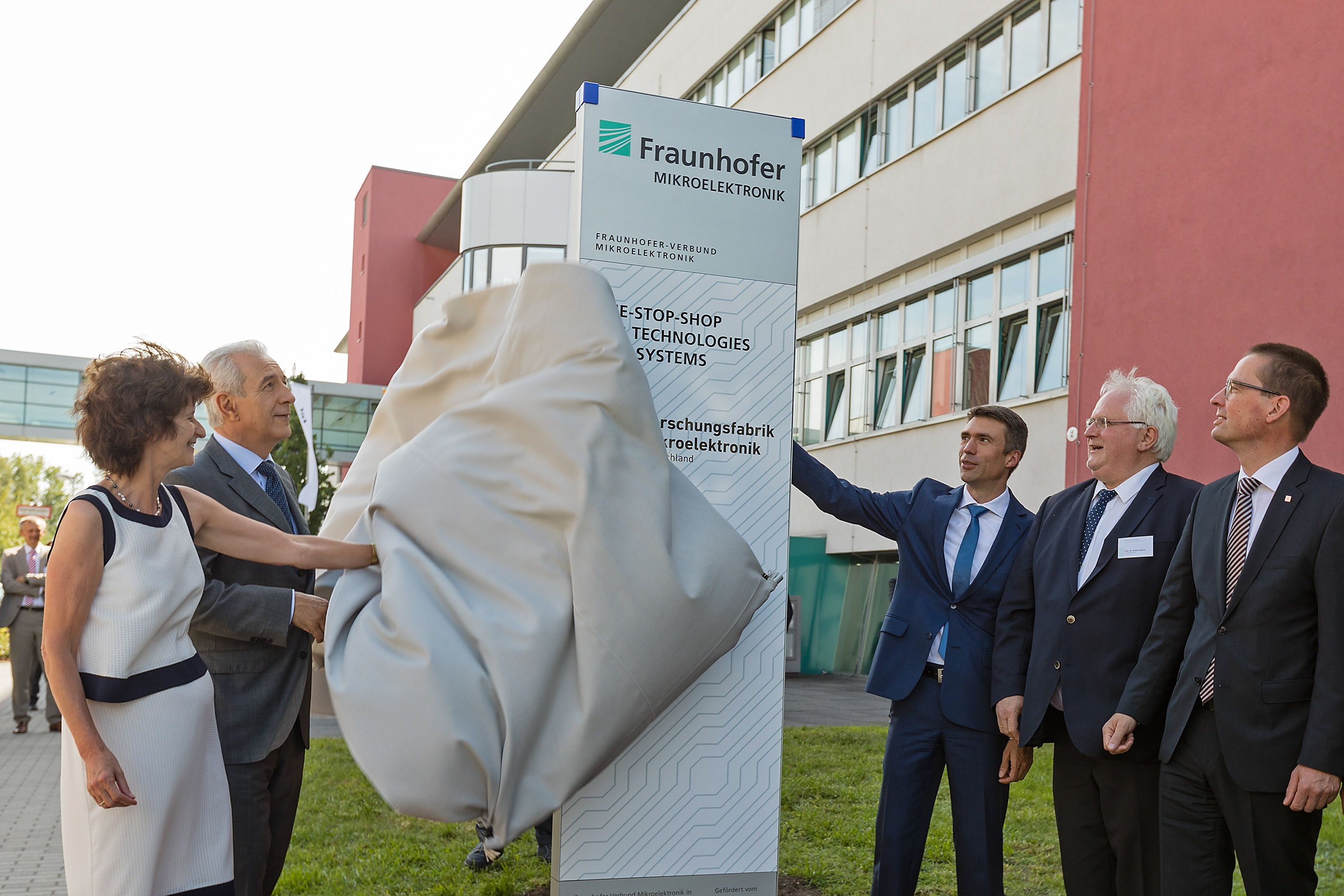
With 200 guests from industry, politics and research, the work of the four Fraunhofer institutes in the Free State of Saxony on the Research Fab Microelectronics Germany will now officially begin. To mark the occasion, Minister President Stanislaw Tillich, Minister of Science Dr. Eva-Maria Stange and Parliamentary State Secretary to the Federal Minister of Education and Research Stefan Müller, together with Prof. Georg Rosenfeld, executive board member at Fraunhofer-Gesellschaft, and the chairman of the steering committee of the Research Fab Microelectronics, Prof. Hubert Lakner, unveiled a column in front of the institute building at the Fraunhofer Institute for Photonic Microsystems.
»Microelectronics is relevant to larger systems,« explains Prof. Rosenfeld. »Established as well as new industries need this technology to master the digital future. With the Research Fab Microelectronics, we are creating the required research equipment and making the know-how available to industry. In this way, the project is making a significant contribution to the technological sovereignty of Germany and Europe.«
Stefan Müller highlighted that, with the Research Fab Microelectronics, Germany will be in a position to advance its own developments in microelectronics better than ever before. »Our future program allows institutes to invest in state-of-the-art, high-performance systems, laboratory equipment and devices in order to offer internationally outstanding research services. In the research fab, we are combining existing research efforts throughout the country into a single excellent pool of know how. We wish not only to produce innovations in the area of microelectronics but also to make them available from a single source across the entire innovation chain. We are therefore strengthening a key industry, including with regard to technology sovereignty, jobs and the attractiveness of Germany as a location for business.«
Minister President Tillich emphasized the importance of Saxony as the leading microelectronics location in Germany and Europe. In his greeting, he stated: »The research fab is giving a further boost to our microelectronics cluster. With an outstanding research landscape, well-educated experts and the close intermeshing of industry and science, Saxony offers the best conditions for employing microelectronics as a key technology for shaping the future of Industry 4.0 as well as for efficient technologies for the energy transition and for intelligent mobility. We therefore support the initiative of the federal government to further strengthen Saxony, Germany and Europe in international competition.«
Minister of Science Dr. Eva-Maria Stange shared a reminder that these large investments are based on structures, such as the service center »Functional integration for micro- and nanoelectronics« in Dresden/Chemnitz, that were built by the Free State of Saxony. »With years of preparations, Saxony has laid the groundwork for the creation of the Research Fab Microelectronics. At the Maria-Reiche-Straße site alone, 128 million euros of structural fund subsidies have flowed into construction projects and the procurement of initial equipment. I am very pleased that our mutual investments in the basic and applied research are now paying off in this way. The Research Fab Microelectronics proves the value of this long but very successful path,« says the minister.
Exactly what this intermeshing of expertise that today is distributed among the application-oriented microelectronics institutes could look like at Fraunhofer was clearly explained by Prof. Hubert Lakner, taking the development of FD-SOI (Fully Depleted Silicon On Insulator) processes on 300 mm wafers as an example. »With the FMD, we can offer the newest technologies along the entire value creation chain, from design to technology modules to wafer-level technologies, including in the leading edge technology range at 300 mm wafers. We are therefore creating interesting offerings for our industry partners for the further development of such high-performance processes in order to bring products to market faster with shorter innovation cycles, especially in the area of the Internet of Things. Our sincerest gratitude goes out to the Federal Ministry for Education and Research for these new possibilities.«
Dr. Rutger Wijburg, who represented the semiconductor and electronics industry at the kick-off event as the CEO of Globalfoundries Dresden, confirmed that excellent high-tech research in the immediate vicinity is a clear advantage for the region. »Globalfoundries has worked successfully with the Fraunhofer company for years. The FMD investment opens up even more excellent opportunities for intensifying and expanding this cooperation. The focus lies on our FD-SOI technology, which is ideal for energy-efficient IoT solutions. With the support of Fraunhofer, we in Dresden are striving to realize the potential of FD-SOI power saving technology on the German and European markets.«
 Fraunhofer Institute for Integrated Circuits IIS, Division Engineering of Adaptive Systems