Newsletter 02/2023
Santa Clara, US, and Dresden, Germany: Collaboration to develop an eFPGA-capable chiplet solution for the next generation of chip-to-chip connectivity technologies

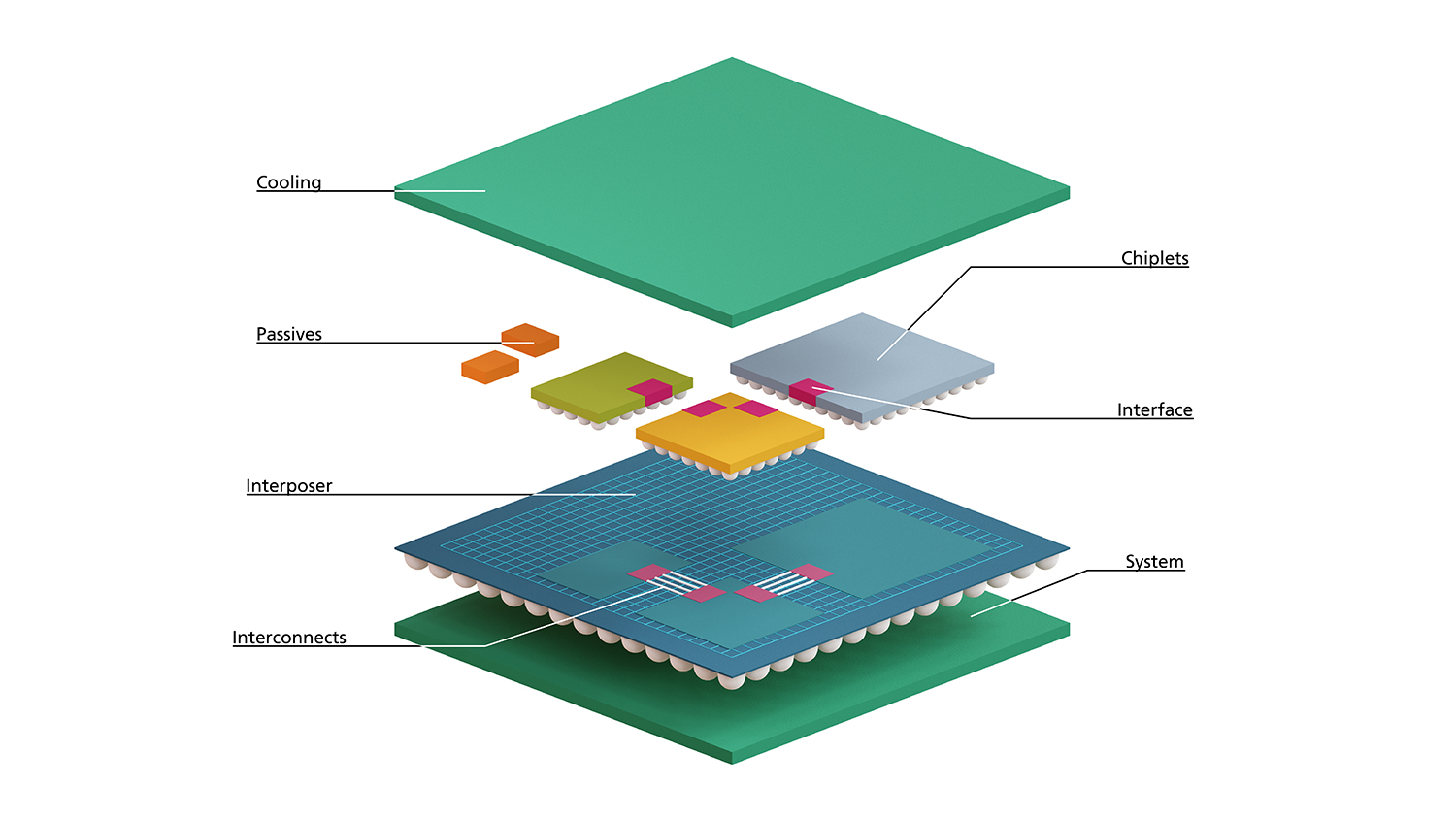
Fraunhofer IIS/EAS and the Achronix Semiconductor Corporation have established a collaboration to develop pioneering semiconductor solutions. The design of state-of-the-art packaging solutions is a focus of research at Fraunhofer IIS/EAS, and Achronix is a leading provider of high-end FPGAs and eFPGA IP solutions. This collaboration aims to create a heterogenous chiplet design capable of demonstrating the performance and interoperability of future high-performance system solutions. Fraunhofer IIS/EAS is contributing its expertise in system concepts, design services and prototyping for cutting-edge packaging designs. In conjunction with Achronix’s Speedcore™ eFPGA IP solution, the partners will create a multi-chip system solution made up of several chiplets. These chiplets make it possible to test and evaluate chip-to-chip transaction layer connections such as Bunch of Wires (BoW) and Universal Chiplet Interconnect Express (UCIe).
The partners believe that chiplet technology is on the cusp of realizing its vast potential for industrial application through a variety of high-performance, heterogeneous multi-chip solutions. The benefit of this technology is that it offers shorter latency times, wider bandwidths and lower costs than individual components connected by conventional conducting paths on a single circuit board. A key application highlighted by the current collaboration project is the connection of high-speed ADCs with Achronix’s eFPGA IP for preprocessing in radar systems and for wireless and optical communication. Achronix’s Speedcore eFPGA IP plays an important role in this application: it offers short latency times as well as reconfigurability while delivering high-performance data acceleration – a must for a great many sophisticated applications.
The collaboration’s goal is to produce a demonstration platform suitable for applications such as 5G/6G wireless infrastructure, ADAS and powerful testing and measuring devices. The collaboration’s specialist insights will be of interest to all players in the semiconductor market striving to achieve interface compatibility in their chiplet projects.
 Fraunhofer Institute for Integrated Circuits IIS, Division Engineering of Adaptive Systems EAS